Reported by Prof. Yi Pan
Center for Spintronics and Quantum Systems
The single- and few-layer Transition Metal Dichalcogenides (TMDs) are promising candidates for post-silicon electronics and optoelectronics. One of the advantages for TMDs, over the other 2D materials, is that each member of the family shows slightly different band structure. Therefore, hetero junctions of particular requirement can be easily designed by selecting two TMDs with appropriate band gaps. For example, the type II (staggered) band alignment heterojunction are realized by stacking single-layer WSe2 on MoS2 (MoS2 -WSe2 heterobilayers). However, the local electronic structure of such heterobilayers is still lacking. To this end, Prof. Yi Pan, who recently joined the Center for Spintronics and Quantum Systems directed by Prof. Tai Min, and collaborators in Germany and the US have carried out comprehensive studies on the MoS2-WSe2 system.
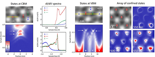
A 2D heterobilayer system consisting of MoS2 and WSe2, grown on epitaxial graphene by means of MOCVD, is investigated by STM/STS at temperatures of 5 and 80 K. A moiré pattern arising from lattice mismatch of 3.7% between the MoS2 and WSe2 is observed. Scanning tunneling spectra (STS) show significant energy shifts of the band edges at the maxima of the moiré corrugation, as compared with STS obtained at corrugation minima. Furthermore, at the minima of the moiré corrugation, sharp peaks in the spectra at energies near the band edges are observed for spectra acquired at 5 K. The peaks correspond to discrete states that are confined within the moiré unit cells. Conductance mapping is employed to reveal the detailed structure of the wave functions of the states, as well as the ordered hexagonal array of such states. For measurements at 80 K, the spectra and conductance maps show less detail due to thermal fluctuation, but confirm that the states are still there. These results indicate that the when future TMDs devices are scaled below 10 nm, the effects of such confined states at the band edges must be taken into account.
The experiment was carried out by Yi Pan, Stefan Fölsch and Prof. Randall Feenstra in Paul Drude Institute. The samples are supplied by Prof. Joshua Robinson’s group in the Pennsylvania State University. The DFT calculations are performed by Prof. Kyeongjae Cho’s group in UT Dallas.
The work is recently published as an article entitled “Quantum-Confined Electronic States Arising from the Moiré Pattern of MoS2-WSe2 Heterobilayers” on Nano Letters, 2018, 18, 1849–1855.
The paper is accessed by https://pubs.acs.org/doi/full/10.1021/acs.nanolett.7b05125
Group website: http://gr.xjtu.edu.cn/web/yi.pan